(China (Mainland))

Product Summary
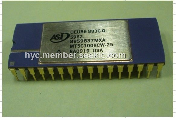
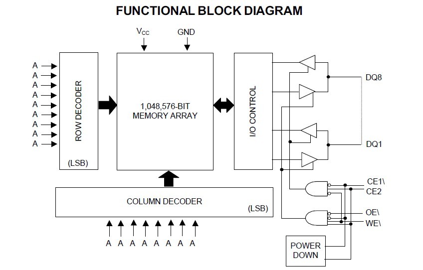
The MT5C1008CW25/883C 128K x 8 SRAM employs high-speed, low power CMOS designs using a four-transistor memory cell, and are fabricated using double-layer metal, double-layer polysilicon technology. For design flexibility in high-speed memory applications, this device offers dual chip enables (CE1\, CE2) and output enable (OE\). These control pins of MT5C1008CW25/883C can place the outputs in High-Z for additional flexibility in system design. The MT5C1008CW25/883C operates from a single +5V power supply and all inputs and outputs are fully TTL compatible.
Parametrics
MT5C1008CW25/883C absolute maximum ratings: (1)Supply Voltage Range (Vcc): -0.5V to +6.0V; (2)Storage Temperature: -65℃ to +150℃; (3)Short Circuit Output Current (per I/O): 20mA; (4)Voltage on any Pin Relative to Vss: -0.5V to Vcc+1V; (5)Max Junction Temperature: +150℃; (6)Power Dissipation: 1W.
Features
MT5C1008CW25/883C features: (1)High Speed: 12, 15, 20, 25, 35, 45, 55 and 70 ns; (2)Battery Backup: 2V data retention; (3)Low power standby; (4)High-performance, low-power CMOS process; (5)Single +5V (+10%) Power Supply; (6)Easy memory expansion with CE1\, CE2, and OE\options.; (7)All inputs and outputs are TTL compatible.
Diagrams
 |
 MT5C 1008 |
Other |
|
Data Sheet |
Negotiable |
|
||||
|
MT5C2564 |
Other |
|
Data Sheet |
Negotiable |
|
||||
|
MT5C2565 |
Other |
|
Data Sheet |
Negotiable |
|
||||
|
MT5C2568 |
Other |
|
Data Sheet |
Negotiable |
|
||||
|
MT5C6401 |
Other |
|
Data Sheet |
Negotiable |
|
||||
|
MT5C6408 |
Other |
|
Data Sheet |
Negotiable |
|
||||