(China (Mainland))

Product Summary
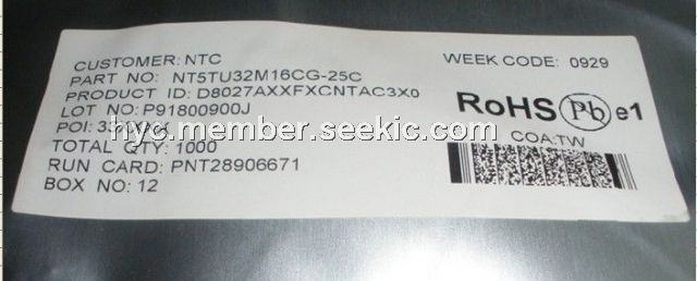
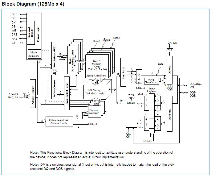
The NT5TU32M16CG-25C is a 512Mb Double-Data-Rate-2 (DDR2) DRAM. It is a high-speed CMOS Double Data Rate 2 SDRAM containing 536,870,912 bits. It is internally configured as a quad-bank DRAM. The NT5TU32M16CG-25C is organized as either 32Mbit x 4 I/O x 4 bank, 16Mbit x 8 I/O x 4 bank or 8Mbit x 16 I/O x 4 bank device. The NT5TU32M16CG-25C is designed to comply with all key DDR2 DRAM key features: (1) posted CAS with additive latency, (2) write latency = read latency -1, (3) normal and weak strength data-output driver, (4) variable data-output impedance adjustment and (5) an ODT (On-Die Termination) function.
Parametrics
NT5TU32M16CG-25C absolute maximum ratings: (1)VDD,Voltage on VDD pin relative to VSS: -1.0 to + 2.3 V; (2)VDDQ, Voltage on VDDQ pin relative to VSS: -0.5 to + 2.3 V; (3)VDDL, Voltage on VDDL pin relative to VSS: -0.5 to + 2.3 V; (4)VIN, VOUT, Voltage on any pin relative to VSS: -0.5 to + 2.3 V; (5)TSTG, Storage Temperature: -55 to + 100℃.
Features
NT5TU32M16CG-25C features: (1)1.8V ± 0.1V Power Supply Voltage; (2)Programmable CAS Latency: 3, 4, 5, and 6; (3)Programmable Additive Latency: 0, 1, 2, 3, and 4; (4)Write Latency = Read Latency -1; (5)Programmable Burst Length: 4 and 8; (6)Programmable Sequential / Interleave Burst; (7)OCD (Off-Chip Driver Impedance Adjustment); (8)ODT (On-Die Termination); (9)4 bit prefetch architecture; (10)Data-Strobes: Bidirectional, Differential; (11)4 internal memory banks; (12)Strong and Weak Strength Data-Output Driver; (13)Auto-Refresh and Self-Refresh; (14)Power Saving Power-Down modes; (15)7.8 μs max. Average Periodic Refresh Interval; (16)RoHS Compliance.
Diagrams
 |
 NT5TU32M16AG-37B |
Other |
|
Data Sheet |
Negotiable |
|
||||