(China (Mainland))

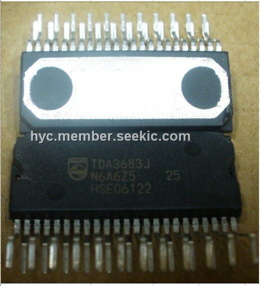
Product Summary
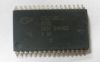
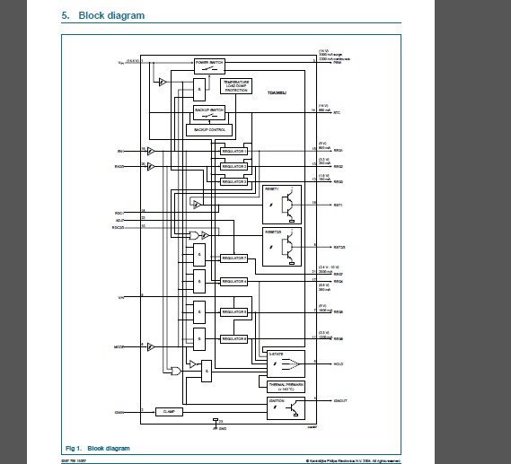
The TDA3683J is a multiple output voltage regulator with a power switch and an ignition buffer. Several protections and diagnostic options are incorporated in this design. The TDA3683J is primarily developed to cover the complete power supply requirements in car radio applications The TDA3683J is especially designed to supply digital circuitry that has to be permanently connected e.g. CAN bus, DPS core and the microcontroller. In combination with the reset delay capacitor (RDC1 or RDC2/3) and the reset function (RST1 or RST2/3), a proper start-up sequence for a microcontroller is guaranteed. The storage capacitor (STC) makes the standby regulator outputs insensitive for short battery drops (e.g. during engine start-up). The switched regulators (regulators 4, 5, 6 and 7) are intended to be used as supply for the tuner, logic, sound processor and CD / tape control The power switch (PSW) can be used for switching the electrically powered antenna, display unit and CD / tape drives The ignition buffer (IGN) is intended to produce a clean logic output signal when a polluted ignition key signal is used as input.
Parametrics
TDA3683J absolute maximum ratings: (1)Tstg storage temperature non-operating -55 +150 °C; (2)Tamb ambient temperature operating -40 +85 °C; (3)Tj junction temperature operating -40 +150 °C; (4)VP1 supply voltage 1 operating: 18 V; (5)VP1 supply voltage 1 reverse polarity; non operating: 18 V; (6)VP1 supply voltage 1 jump start; t ≦ 10 minutes: 30 V; (7)VP1 supply voltage 1 load dump protection; t ≦50 ms; tr ≧2.5 ms: 50 V.
Features
TDA3683J features: (1)Three enable pin controlled standby regulators: REG1: 5 V / 600 mA controlled by the EN1 input, REG2: 3.3 V / 200 mA controlled by the EN2/3 input, REG3: 1.9 V / 150 mA controlled by the EN2/3 input; (2)Four mode pin controlled switched regulators: REG4: 8.5 V / 350 mA, REG5: 5 V / 1.8 A, REG6: 3.3 V / 1.2 A, REG7: 2.4 V to 10 V / 2 A adjustable using external resistor divider; (3)One mode pin controlled power switch; 2.2 A continuous and 3 A surge, with delayed lower current limit so as to be less sensitive to inrush currents; (4)One independent ignition buffer (inverted output, open-collector)with good input protection against high transients; (5)A storage capacitor is included to provide back-up supply for the standby regulators in the event of loss of battery supply.
Diagrams
| Image | Part No | Mfg | Description |  |
Pricing (USD) |
Quantity | ||||||||||||
|---|---|---|---|---|---|---|---|---|---|---|---|---|---|---|---|---|---|---|
 |
 TDA3683J/N2C |
NXP Semiconductors |
Linear Regulators - Standard MULTIPLE VOLTAGE REGULATOR |
Data Sheet |
Negotiable |
|
||||||||||||
|
TDA3683J/N2C,112 |
NXP Semiconductors |
Linear Regulators - Standard MULTIPLE VOLTAGE |
Data Sheet |
Negotiable |
|
||||||||||||
|
TDA3683J/N2S,112 |
NXP Semiconductors |
Linear Regulators - Standard MULT VLTG REGULATOR SWITCH/IGNITION BUFF |
Data Sheet |
|
|
||||||||||||