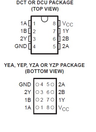
Product Summary
The SN74LVC2G32DCUT is a dual 2 input positive—or gate. This device is fully specified for partial—power—down applications using Ioff. The Ioff circuitry disables the outputs, preventing damaging current backflow through the device when it is powered down.
Parametrics
SN74LVC2G32DCUT absolute maximum ratings: (1)Supply voltage range, VCC: —0.5 V to 6.5 V; (2)Input voltage range, VI (see Note 1): —0.5 V to 6.5 V; (3)Voltage range applied to any output in the high-impedance or power-off state, VO (see Note 1): —0.5 V to 6.5 V; (4)Voltage range applied to any output in the high or low state, VO (see Notes 1 and 2): —0.5 V to VCC + 0.5 V; (5)Input clamp current, IIK (VI < 0): —50 mA; (6)Output clamp current, IOK (VO < 0): —50 mA; (7)Continuous output current, IO: ±50 mA; (8)Continuous current through VCC or GND: ±100 mA; (9)Package thermal impedance, θJA (see Note 3): DCT package: 220°C/W.
Features
SN74LVC2G32DCUT features: (1)Supports 5-V VCC Operation; (2)Inputs Accept Voltages to 5.5 V; (3)Max tpd of 3.8 ns at 3.3 V; (4)Low Power Consumption, 10-μA Max ICC; (5)±24-mA Output Drive at 3.3 V; (6)Typical VOLP (Output Ground Bounce)<0.8 V at VCC = 3.3 V, TA = 25°C; (7)Typical VOHV (Output VOH Undershoot)>2 V at VCC = 3.3 V, TA = 25°C; (8)Ioff Supports Partial-Power-Down Mode Operation; (9)Latch-Up Performance Exceeds 100 mA Per JESD 78, Class II.
Diagrams

| Image | Part No | Mfg | Description |  |
Pricing (USD) |
Quantity | ||||||||||||
|---|---|---|---|---|---|---|---|---|---|---|---|---|---|---|---|---|---|---|
 |
 SN74LVC2G32DCUT |
 Texas Instruments |
 Gates (AND / NAND / OR / NOR) Dual 2 Input Pos OR Gate |
 Data Sheet |

|
|
||||||||||||
 |
 SN74LVC2G32DCUTE4 |
 Texas Instruments |
 Gates (AND / NAND / OR / NOR) Dual 2 Input Pos OR Gate |
 Data Sheet |

|
|
||||||||||||
 |
 SN74LVC2G32DCUTG4 |
 Texas Instruments |
 Gates (AND / NAND / OR / NOR) Dual 2 Input Pos OR Gate |
 Data Sheet |

|
|
||||||||||||
 (China (Mainland))


